 We have worked on a myriad of processes for production of semiconductor and optical materials, from melt, solution, and vapor. The materials we have worked on include elemental (Si, Ge), compound III-V (GaAs, InGaAs, InP), compound II-VI (CdTe, CdZnTe, HgCdTe, MnCdTe), Wide Band Gap Materials (SiC, AlN, AlGaN), and optical materials (CaF2, NaI2).
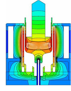
In one example, a producer of electronic materials wanted to modify its crystal growth furnaces to increase production yield. We created a comprehensive model for the crystal growth process and simulated the effect of planned hardware modifications on heat transfer in the equipment. Our tools were used to optimize the growth process and achieve the increased process yield. The modified furnaces are now routinely used in large volume production.
|
